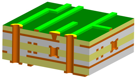
High-Density Interconnect PCBs (HDI PCBs) deliver a significantly higher wiring density than standard through-hole PCBs, enabling innovative and compact electronic designs. As outlined by IPC-6012 standards, these PCBs provide 20 or more electrical connections per square centimetre on each side, making them ideal for sophisticated and space-saving applications.


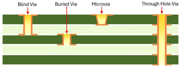
The HDI approach allows for the creation of smaller, lighter, and highly reliable electronic products by integrating advanced features such as multiple layers, precise traces, microvias, and blind or buried vias. With HDI technology, shorter signal pathways reduce power loss and enhance electrical performance. This makes HDI PCBs essential for high-speed signals and applications requiring exceptional signal integrity in cutting-edge industries.
Key Characteristics of HDI PCBs
HDI PCBs adhere to IPC-2226 guidelines, incorporating design elements that enhance their functionality:

HDI PCBs represent a key advancement in PCB technology, meeting the growing demand for compact, high-performance electronics in sectors like telecommunications, aerospace, automotive, and medical devices. Their innovative design features and exceptional electrical performance make them an essential solution for modern electronic applications. If you're seeking high-quality HDI PCBs tailored to your specific requirements, get in touch with our team at TCL to discuss your project.
HDI Capabilities
| Feature | Technical Specification |
|---|---|
| Max Layer Count | 22, advanced 50 |
| PCB Thickness | 0.3mm - 4.5mm |
| PCB Size | 50 x 50mm - 700 x 600mm |
| Max Copper Thickness | Outer layer:6OZ Inner layer: 6OZ |
| Minimum Hole Size | 0.1mm, advanced 0.075MM |
| Max Hole Size | 3.5mm |
| Tighest Hole Tolerence | PTH:±0.075MM, NPTH:±0.05MM |
| Min Track Width | 0.762mm |
| Min Gap | 0.762mm |
| Finishes | OSP, ENIG, ENEPIG, EPAG, Immersion tin, Immersion Silver |
HDI Sample