español

PCB's with Embedded Components

Embedded components in PCBs

At TCL, we’re passionate about pushing the boundaries of PCB technology to meet the evolving needs of our customers. A key innovation in this area is embedding semiconductor dies and CoolMOS packages directly into the PCB - offering exciting possibilities beyond traditional approaches.
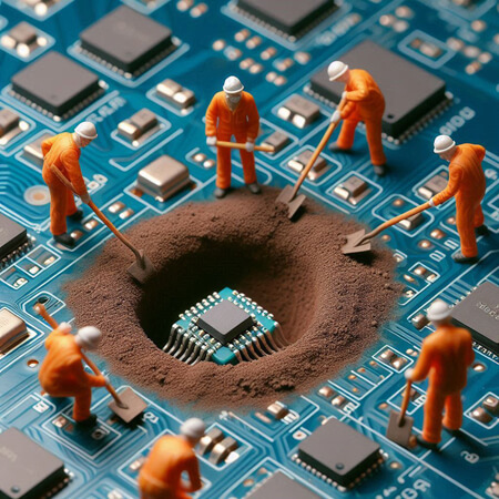
Here’s why this technique is a game-changer:

  • Miniaturisation and Space Efficiency: Embedding components allows for more compact and densely packed designs. This helps reduce the size and weight of products, which is particularly valuable in space-sensitive applications like aerospace and mobile devices.
  • Boosted Voltage Utilisation: By shortening interconnections and optimising the layout of embedded components, signal crosstalk is reduced, improving the utilisation of the device’s voltage capabilities.
  • Lower Parasitic Inductances: Embedding minimises the parasitic inductance and capacitance seen in traditional surface-mount designs, leading to better signal integrity and overall performance.
  • Improved EMI Performance: Reducing electromagnetic emissions through embedding enhances electromagnetic compatibility (EMC), helping devices meet stringent standards.
PCB with embedded components

By embedding components directly into the PCB, we not only improve performance and reliability but also open the door to greater design flexibility and potential cost savings. It’s an approach that’s particularly useful for high-performance and space-constrained applications.

While we can’t share specific project details due to NDAs, our Technical Sales Team is always available to discuss how we can help bring these innovations into your next project.

Contact TCL Elektronika now to discuss your next project